
Bosstone Build Guide
This circuit has been simulated but not built yet. The connections were reconstructed from published clone parts lists and still need checking against a reference schematic. The voltages in this guide are simulated, not measured. Try it on a breadboard before you commit to stripboard.
Assembly Procedure
Prepare your workspace
Find a clean, well-lit area to work. You will need the following:
- Soldering iron and flux-core solder
- Small wire cutters and wire strippers
- Multimeter (you use it to check cuts, parts, and voltages)
- A 3 mm (1/8 in) drill bit or a stripboard track cutter
- Heat gun or lighter for heat-shrink tubing
- Helping hands, or similar device, to hold parts while soldering
Gather the parts
The Bosstone is a high-gain NPN stage (Q1) followed by a PNP buffer (Q2), then clipping diodes. A three-way toggle picks 1N4148 silicon diodes, no diodes, or two LEDs.
Count Part Value Notes 1 Stripboard 18 × 8 holes 0.1 in pitch, strips along the 18-hole length 1 Transistor, Q1 2N2222 (NPN) Or 2N3904, BC337-25, S8050-D 1 Transistor, Q2 2N3906 (PNP) Or BC327, S8550, A1015 1 Resistor, R1 150 kΩ (brown, green, yellow) 2 Resistors, R2 and R3 560 kΩ (green, blue, yellow) 2 Resistors, R4 and R5 18 kΩ (brown, gray, orange) 3 Film capacitors, C1, C2, and C4 22 nF (223) 1 Ceramic capacitor, C3 47 pF (470) 2 Diodes, D1 and D2 1N4148 2 LEDs, D3 and D4 Same color, so both halves of the wave clip alike 1 Potentiometer, ATTACK B100k 16 mm, linear 1 Potentiometer, VOLUME A100k 16 mm, audio (log) 1 Toggle switch, CLIP SPDT on-off-on 1 3PDT footswitch 9 solder lugs 1 LED and bezel 5 mm Effect-on indicator 1 LED resistor 4.7 kΩ (yellow, violet, red) 2 1/4 in jacks Stereo (input), mono (output) 1 9 V battery snap — Hookup wire, link wire, heat-shrink tubing Try it on a breadboard (recommended)
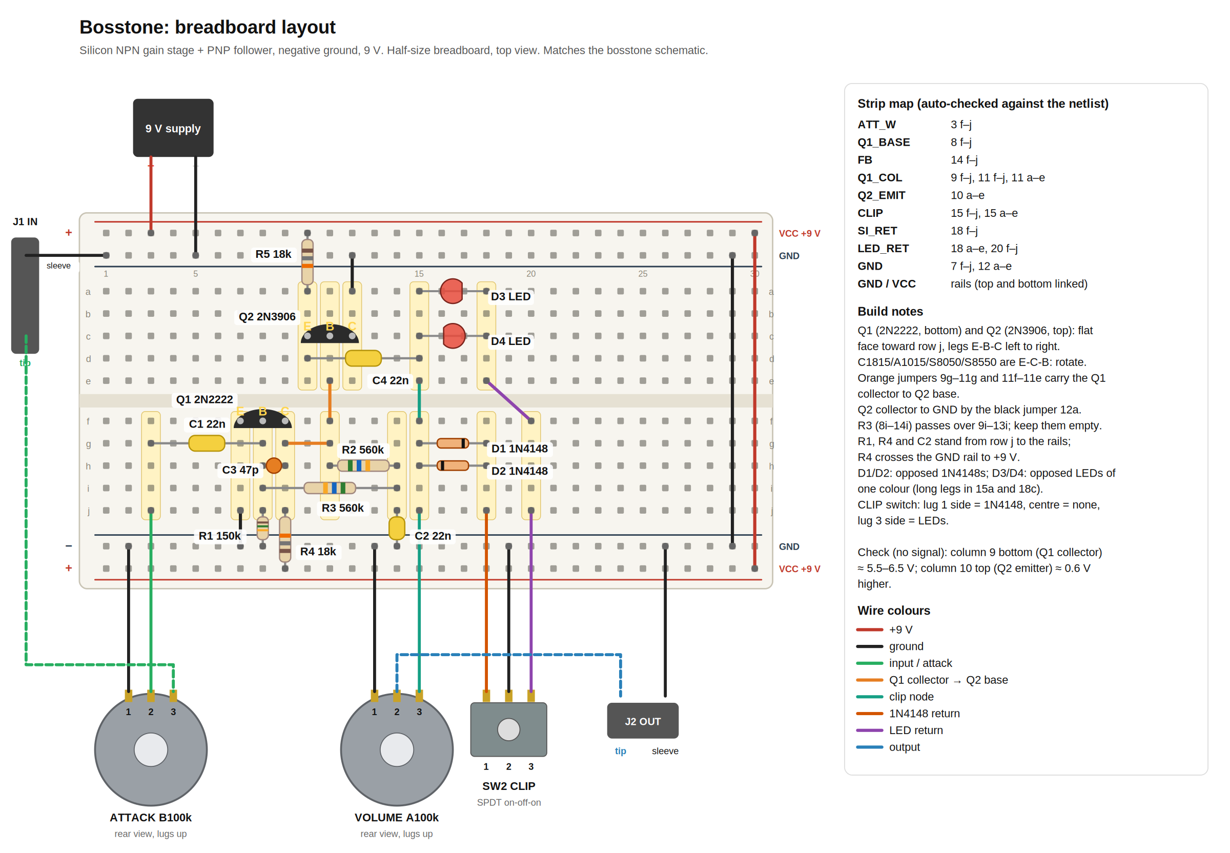
Because the connections in this design haven't been confirmed on a working pedal, build it on a half-size breadboard first. The breadboard layout wires the jacks straight to the circuit, without the footswitch. Select the diagram to open the full-size image.
Learn the board
Stripboard has copper strips running along its length. Every hole in a strip is connected, so the strips do the wiring for you. You break a strip where two parts must not connect.
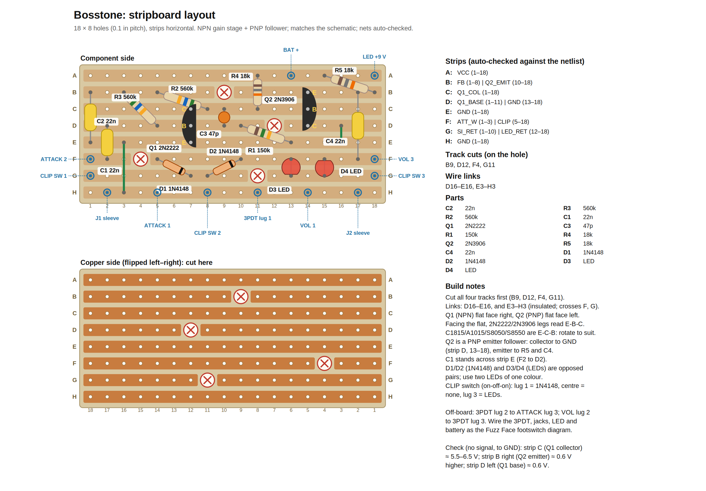
Holes are named by row and column. Rows run A to H from top to bottom, and columns run 1 to 18 from left to right, with the parts on top and the copper underneath. For example, D16 is row D, column 16. Keep the layout diagram open while you work.
 ImportantThe copper side is a mirror image
When you flip the board over to cut or solder, left and right swap. Column 1 is now on your right. The layout's copper-side view is already flipped for you, so use that view whenever the copper is facing up.
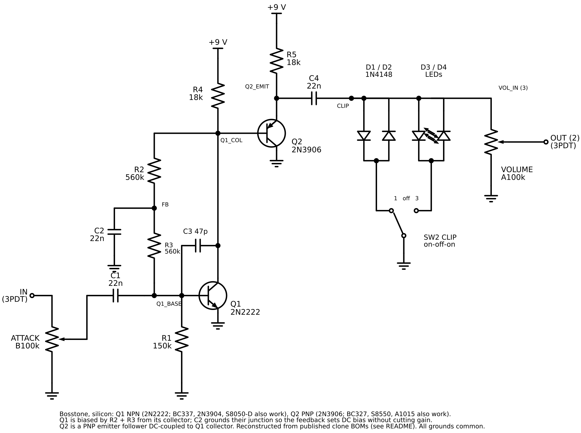
The schematic shows the same circuit. It's useful when you check voltages or trace a fault.
Cut the tracks
Four holes need their copper cut: B9, D12, F4, and G11. Cut the tracks before you install any parts.
Mark the cuts
With the copper side up, find each cut on the copper-side view and mark it with a fine marker. Count columns from the right-hand edge, because the board is flipped.
Cut each hole
Place the drill bit in the marked hole and twist it by hand, with light pressure, until the copper ring around the hole is gone. You only need to cut through the copper, not through the board.
Check every cut
Set your multimeter to continuity. Check B8 to B10, D11 to D13, F3 to F5, and G10 to G12. None may beep. If one beeps, a sliver of copper remains: twist the bit again, or scrape the gap with a hobby knife.
Install the wire links
- D16 to E16: bare wire is fine. It grounds Q2's collector strip.
- E3 to H3: use insulated wire. It crosses strips F and G, and it must not touch them.
Solder both ends and trim the excess on the copper side.
Install the resistors
Resistors are not polarized. For each one, bend the leads to fit the holes, push it flat against the board, solder, and trim. Check each value with your multimeter before you solder it.
Resistor Value Holes R3 560 kΩ B3 to D5 (diagonal) R2 560 kΩ B5 to C8 (diagonal) R1 150 kΩ D10 to E13 (diagonal) R4 18 kΩ A11 to C11 (crosses strip B) R5 18 kΩ A15 to B18 (diagonal) Install the clipping diodes
D1 and D2 face opposite ways, so one clips the top of the wave and the other clips the bottom. D3 and D4 do the same. The band on a 1N4148 marks its cathode. On an LED, the short lead is the cathode.
Diode Anode Cathode D1 (1N4148) F5 G7 (band) D2 (1N4148) G8 F10 (band) D3 (LED) F13 (long lead) G13 (short lead) D4 (LED) G15 (long lead) F15 (short lead) CautionCheck each pair is opposedIf both diodes in a pair face the same way, that switch position clips only one half of the wave and sounds lopsided. Check the bands and short leads against the table before you solder.
Install the capacitors
None of these capacitors is polarized.
- C3 (47 pF ceramic): C9 to D9.
- C2 (22 nF film): B1 to E1.
- C1 (22 nF film): D2 to F2. It stands over strip E, which it doesn't connect to.
- C4 (22 nF film): B17 to F17.
Install the transistors
Install the transistors last, because they are the most heat-sensitive parts. Work quickly: about 2 seconds per joint, and let the part cool between joints.
Transistor Flat face points Holes Q1 (NPN) Right (toward column 18) C in C7, B in D7, E in E7 Q2 (PNP) Left (toward column 1) E in B14, B in C14, C in D14 CautionQ1 and Q2 are different types and face opposite waysQ1 is the NPN and Q2 is the PNP. Swapping them, or installing one backwards, is the most likely mistake in this build. Match each one to the layout diagram before you solder.
CautionCheck the pinout of your transistorsWhen you look at the flat face with the leads pointing down, a TO-92 2N2222, 2N3904, 2N3906, BC337, or BC327 reads E, B, C from left to right. A C1815, A1015, S8050, or S8550 reads E, C, B. With an E-C-B part, bend or rotate it so each lead still lands in the hole the table gives for that lead. A metal-can 2N2222 has a different pinout: check its datasheet.
Attach the off-board wires
Solder a wire into each pad below from the component side, long enough to reach its part in the case. Leave some slack.
Pad Goes to Suggested color A13 Battery snap + Red A18 LED resistor, then the LED's long lead Red F1 ATTACK lug 2 Green F18 VOLUME lug 3 Blue G1 CLIP switch lug 1 Yellow G18 CLIP switch lug 3 Yellow H2 Input jack sleeve Black H5 ATTACK lug 1 Black H8 CLIP switch lug 2 (middle) Black H11 Footswitch lug 1 Black H14 VOLUME lug 1 Black H17 Output jack sleeve Black Pot lugs are numbered 1, 2, 3 from left to right when you look at the back of the pot with its lugs pointing up.
Wire the footswitch, jacks, and LED
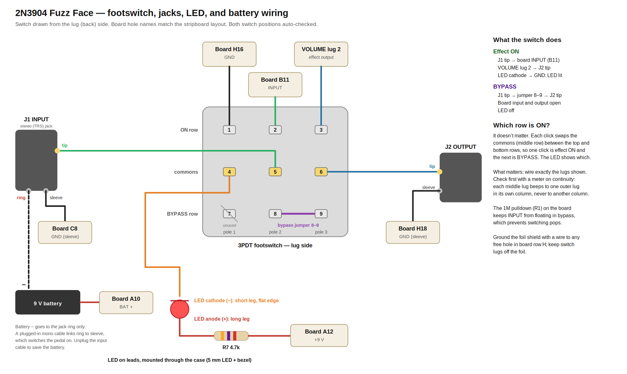
The footswitch wiring is the same as the Fuzz Face kit's, except that footswitch lug 2 goes to the ATTACK pot instead of the board. The diagram shows Fuzz Face hole names, so use the pad table above for the board end of each wire. Select the diagram to open the full-size image.
Check the footswitch
With your meter on continuity, check that each middle-row lug beeps to exactly one outer lug in its own column. Click the switch and check again: it should now beep to the lug at the other end of the same column.
Wire the footswitch
- Lug 2 to ATTACK lug 3.
- Lug 3 to VOLUME lug 2.
- Lug 5 (middle) to the input jack tip.
- Lug 6 (middle) to the output jack tip.
- Lug 8 to lug 9: a short bare jumper. This is the bypass path.
- Lug 1 already has a wire from the board. Lug 7 stays empty.
Wire the LED
Solder the LED resistor to the LED's long lead (anode, +), and the wire from pad A18 to the resistor's other end. Solder a wire from the LED's short lead (cathode, −) to footswitch lug 4. Cover the joints with heat-shrink tubing.
Wire the battery
Solder the battery snap's red lead to pad A13. Solder the black lead to the input jack's ring lug, not to the board. A mono plug in the input jack connects the ring to the sleeve, so the pedal only draws power while a cable is plugged in.
Verify the build
Before you connect a battery, inspect and test the assembly.
Inspect the copper side
Check every joint. Joints should be shiny and smooth, with no solder bridging two strips. Most stripboard faults are a solder bridge or a missed cut.
Check for a short
With no battery connected, measure the resistance between pad A13 (+9 V) and any hole in row H (ground). It must not read close to 0 Ω.
Check the clipping switch
On continuity, check that pad H8 beeps to G1 with the toggle one way, to G18 the other way, and to neither in the middle.
Check the voltages
Connect the battery, plug a cable into the input jack, and put the black probe on any hole in row H. With no guitar signal, measure:
Point Expected (simulated) Strip A (+9 V) About 9 V Strip C (Q1's collector, Q2's base) About 6.3 V (5.5 to 6.5 V is fine) Strip B, columns 10 to 18 (Q2's emitter) About 6.95 V, about 0.6 V above strip C Strip B, columns 1 to 8 (bias feedback) About 3.45 V Strip D, columns 1 to 11 (Q1's base) About 0.6 V If these readings are far off, or the pedal doesn't work, compare the board with a reference Bosstone schematic as well as checking for build faults. Note anything you change, so the layout can be corrected.
Test it
Connect your guitar to the input and your amplifier to the output. Start with the amplifier quiet.
- Click the footswitch until the LED is off. You should hear your clean guitar.
- Click again. The LED lights and you should hear the fuzz.
- Try all three CLIP positions, and turn ATTACK and VOLUME through their full range.
CautionThe middle CLIP position is much louderWith no diodes in circuit, nothing limits the output level. Turn VOLUME down before you switch to the middle position.
Mount it in the case
Mount the footswitch, both pots, the toggle, both jacks, and the LED bezel, and tighten their nuts. Put standoffs or insulating tape on the copper side of the board, then fit it in the case. Place the battery where its terminals can't touch the board or the switch lugs. Close the case and test again.
CautionKeep bare metal off the caseIf you line the case with foil tape, any bare lead or joint that touches it causes a short. Ground the foil with a wire to any free hole in row H.
Operating Instructions
The Bosstone is an aggressive, buzzy fuzz with a thin low end. ATTACK sets how hard your signal hits the gain stage, VOLUME sets the output level, and the CLIP toggle picks the clipping:
- 1N4148 diodes: the most compressed, and the quietest.
- Middle (no diodes): only the transistors clip. The loudest and most raw setting.
- LEDs: between the two. Louder and more open than the 1N4148s.
The toggle's lever connects the middle lug to the lug at the opposite end, so mark which way is which after you test it. The footswitch switches between the effect and true bypass, and the LED is lit when the effect is on. The pedal draws power only while a cable is plugged into the input jack.
Troubleshooting
- Bypass works, but there's no sound with the effect on: check that the guitar goes into the input (stereo) jack, and that footswitch lug 2 goes to ATTACK lug 3.
- Strip C reads close to 9 V: Q1 isn't conducting. Check its pinout and direction, R2 and R3, and the cut at D12.
- Strip C reads under 1 V: look for a solder bridge between strip C and strip D.
- Strip B, columns 10 to 18, reads close to 9 V: Q2 isn't conducting. Check that it's the PNP, its direction, and the D16 to E16 link.
- The LED position sounds the same as the 1N4148 position: the cut at G11 is missing or bridged.
- A diode position is as loud as the middle position: that pair's wire to the toggle is loose.
- The LED doesn't light: the LED is probably backwards. Its short lead goes to footswitch lug 4.